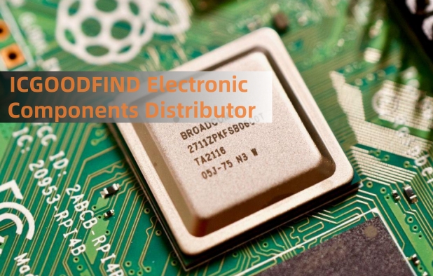
The Intel D8749H stands as a landmark component in the history of computing, representing a crucial step in the evolution of embedded control systems. As a member of the MCS-48 family, it was among the first generation of truly complete microcontrollers, integrating all the critical components of a computer—CPU, RAM, ROM, and I/O—onto a single piece of silicon. This architectural innovation paved the way for the intelligent embedded devices that now permeate our world.
At its core, the D8749H features an 8-bit CPU based on the 8048 architecture, operating at a clock frequency of up to 11 MHz. This central processor was optimized for control-oriented tasks, executing its instruction set efficiently. A key differentiator from simple microprocessors was its integrated memory. The chip contained 2 KB of onboard UV-erasable EPROM (the 8749H variant), which allowed developers to write, test, and erase their firmware with relative ease during the prototyping phase. This was complemented by 128 bytes of on-chip RAM, a significant amount for the era, used for variable storage and system stack operations.
The peripheral set of the D8749H is what truly cemented its role as an embedded controller. It featured:
27 programmable I/O lines, organized into three 8-bit ports (Ports 1 and 2) and one quasi-bidirectional 8-bit bus (Bus Port). This provided ample connectivity for interfacing with sensors, actuators, keyboards, and displays.
A built-in 8-bit timer/counter that could be used for event counting, interval timing, or generating precise baud rates for serial communication.
An single-level interrupt system that could be triggered by an external pin or the internal timer, enabling the microcontroller to respond promptly to real-time external events.
The system was designed for expansion. While it could operate as a standalone single-chip solution, the D8749H could also access up to 2 KB of external program memory and 256 bytes of external data memory, providing flexibility for more complex applications. Its instruction set included over 90 instructions, many of which were single-byte and single-cycle, ensuring compact code and fast execution—a critical requirement for real-time control.

In practice, the D8749H and its siblings became the brains behind a vast array of early embedded systems. Its applications were diverse, ranging from automotive engine control units and industrial automation to keyboards, printers, and early telecommunications equipment. By consolidating numerous discrete logic chips into one package, it dramatically reduced the size, cost, and power consumption of electronic products, accelerating the pace of innovation.
ICGOOODFIND: The Intel D8749H was not merely a chip; it was a foundational platform that demonstrated the power and practicality of the single-chip microcontroller concept. Its integrated architecture of processor, memory, and I/O established a blueprint that would be refined and scaled for decades, making it a true pioneer in the journey towards an interconnected, intelligent world.
Keywords:
1. MCS-48 Architecture
2. Integrated Microcontroller
3. On-Chip EPROM
4. Programmable I/O
5. Embedded Control
